Recent Work.
These are a few examples of recent work we have performed for clients.
Starting with a sucessful project for a defence contractor in 2004 we have
built up close links with Abelon Systems, a local Software
design consultancy company. NSD and Abelon have complimentary skill sets (FPGA &
Hardware development / Embedded and Higher level software development) that
have allowed us to sucessfully complete a number of projects for a variety of
clients over the last few years.
This collaboration has allowed us to jointly undertake larger system level
development projects than we could have undertaken individually, in parallel
with projects that utilise our respective core skill sets.
Synectics Systems
NSD has provided FPGA design and consultancy services, completing an FPGA development project, functional
expansion development and advising on FPGA implementation on a newly designed PCB.
This has lead to repeat work.
Medium Sized Company - Scottish Central Belt
We have developed a NICAM encoder core for this sucessful centrally based Scottish
company. This encompasses digital system design, input frequency compensating and
output spectrum limiting DSP filters and the DQPSK RF back end.
Through careful low level design we have manged to squeexe two cores into a single
EP2C5 CycloneII FPGA. This has to undergo further system tests but is currently working
well.
Local Start Up
In conjunction with Abelon Systems.
We have designed and are developing a complete hardware and software system design for a local
start up. This has included using FPGAs to interface with a very large number of control inputs,
provide PWM control outputs and provide a flexible expandable hardware platform based around
serial interfaces between the various hardware components. This product will operate in an electrically
noisy environment so much attention has been paid to input filtering/protection and isoltation
between the different system modules.
This development is on-going, more details will be released soon.
Aspects Software
In conjunction with Abelon Systems.
See below for further background on Aspects Software.
Knowing that Aspects' old test tools product was coming to the end of its useful life, NSD and Abelon Systems
pitched a product design proposal to Aspects. We were awarded the job and sucessfully completed the
design of the Aspects SS3. NSD
completed all Hardware, FPGA and Mechanical design, Abelon handled the embedded software (on an SBC) and
the PC based web browser controller. The hadware design included a significant portion of analogue design
for which we sought advice from an external consultant. We didn't have time to not get things 95% right first
time.
The SS3 is performing well in the marketplace for Aspects meeting all customer requirements.
This has lead to further work for Aspects in conjunction with Abelon.
Optos PLC
Optos provides a revolutionary laser
scanning retinal imaging device.
We provided FPGA development services during the bring up phase of a new electronic
module design. This also included an electro-mechanical analysis of a system performance
problem, and safety critical work on the laser safety monitoring FPGA.
This has lead to
more recent further FPGA and hardware design work, details will be announced soon.
Defence Contractor
In conjunction with Abelon Systems.
Our client, a major defence contractor, had a requirement to replace some
vital secure communications link equipment which had a number of obsolete
components. This system had been designed in the mid 1980's and the hardware
and many components were becoming un-reliable. The requirement was to bridge
between the 15 year old proprietary link and a standard ethernet LAN
connection. The client had sought a replacement solution around XXX several years
ago but had been told that it could not be done.
The regime of careful/regular maintenance was unable to maintain the
reliability of this old system which was mission critical where it was
installed, a reliable replacement was urgently required. A tender was
submitted in conjunction with Abelon in competition with several notable
suppliers, we were awarded the contract.
The solution is based on an off-the-shelf SBC mounted on a custom PCI
interface board with an Altera Cyclone FPGA. The FPGA cpatures the
propritary link data, storing this for retrieval by the SBC, this then
encapsulates it and passes it on with a TCP/IP stack. The design of the
hardware concentrated on the MTBF and robustness while providing an
upgradeable platform for future requirements. The sofware and FPGA
configuration are remotely field upgradeable.
Only a few days on site were required to install and commission the drop in
replacement for the exisiting equipment. This was remarked upon and compared
to the many weeks required to comission the original system.
The solution has now been running trouble free for three years.
Chorus Motors
We provided FPGA design and hardware design services to
Chorus Motors. This included quickly (2 weeks)
providing a risk reduction FPGA board based on Altera's Cyclone because of initial Xilinx Spartan3 supply
difficulties. The Cyclone board ended up being used and can be seen here
(top right photo). The FPGAs ability to control multiple motor phases is an integral part of the Chorus Motors drive technology.
This is an ongoing partnership, NSD is supporting Chorus as and when further FPGA development is required.
Agilent Technologies
Custom FPGA system design and development.
SDH traffic mapper/generator
At the 'bottom end' the design received raw PDH traffic, from DS1 to E4, and mapped it into the appropriate
Virtual Container (VC). As an example for a Floating Byte Aligned DS1 input this involved
extracting the unaligned frame bits from the serial data stream and byte aligning the remaining
data bits to form the VC11 multi frame.
The VCs could then be packed into any valid TU structure to produce an STM1 output.
Valid and invalid TU pointer burst sequences could be generated. All data and POH error,
and alarm types could be activated at user defineable rates, or asserted permanently.
Tandem connection monitoring could be enabled in the Low Order or High Order path
overheads and all error states and alarms could be generated.
A design specification was written and an architecture designed based on a Product Requirement
Specification which initally only loosely described the design behaviour, the stipulation
that the new product behaviour should mirror the old product (OMNIBerr) behaviour,and
ITU G.707. The software control interface were designed to match existing interfaces
allowing software driver re-use.
Testbenches were written for every sub-module and for the overall design. Integration testing was
performed by hand, and with the aid of Perl scripts/GUI. A
generic debug ram was included in the design to enable live internal traffic to
be captured for debug.
This design was coded and documented to the Agilent standards, and ran at 80MHz
on a Virtex-E600 in the target system.
Module Bridge Design
Implemented the module bridge chip for the 2.5G optics card. Wrote the specification
for, then designed the application logic interfacing with a Xilinx PCI interface core. Implemented
2 serial adc interfaces, serial dac interface and spec'd, designed and implemented a
simple three wire interface for register access of two other FPGAs. Performed board
debug of ADC/DAC interface and drivers. Overcame a hardware fault (3.3v device driving a 5v cmos
clock input) with an external pullup and an IO buffer trick (the rise time with a
simple tristate/pullup was too slow) to allow functional debug of the interface before
a board re-spin. Wrote application notes for the software engineers on driving the ADCs
over the serial interfaces (these were complex to set up/drive). This design was targeted
at a Xilinx SpartanII clocked at 80MHz.
Ethernet IF Board Sub Modules
Designed and implemented an ethernet frame receive/rate change module and field
identification modules for incoming frames. This wasn't trivial as certain
proprietary fields could only be identified once the end of the frame had been received,
the frames were of unknown length and frame latency through this module had to be
constant. These were part of a system design targeted at a Xilinx VirtexII 4000 clocked at
80MHz.
The work above at Agilent Technologies was performed under a series of repeat contracts
which covered the entire period of this new product line development.
Aspects Software
FPGA and Hardware debug and design
Aspects is a medium sized software company based in Edinburgh with a suite of
test tools for the analysis of the comms between a mobile phone and a sim
card, based on a hardware platform. The present evolution of this platform
had been out in the field for approximately one year but has at times behaved
erratically with different clients experiencing different levels of performance,
which sometimes weren't to specified levels.
Our job was to debug the hardare/FPGA design and hopefully extend the performance
to an acceptable level. The system had been selling well worldwide, so a recall
to replace hardware would be expensive. The FPGA could be updated via a new software
release to customers so this was the preferred route for any fixes if possible.
Several different people, none of who were still with Aspects, had worked on the
FPGA/hardware design which was largely uncommented/undocumented. There were no
testbenches or other means of verifying functional behaviour of the designs.
A rough block diagram of the system is shown here.
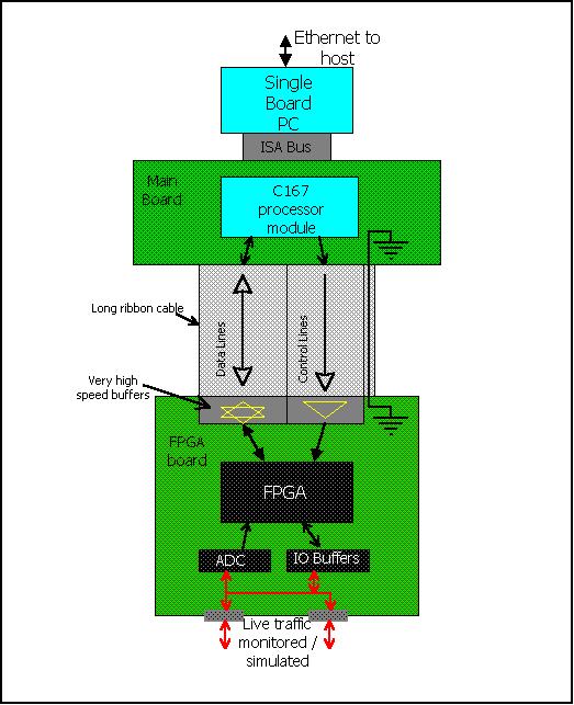
Initial investigations concentrated on the FPGA design and FPGA/uP interface
as large noise spikes had been observed on this interface previously.
The FPGA was clocked at 50MHz, but the P+R tools reported a maximum
speed of 28MHz, together with many warnings of ripple clocks, gated clocks etc.
The uP interface was not synchronous, using the uP WR_n signal to register
data into registers etc (the uP ran asynchronously to the FPGA).
In order to debug the interface the uP interface was re-written as a
synchonous design with all control signals re-timed to the 50MHz clock
domain. With only a dummy traffic generator and the new uP interface
in the FPGA noise spikes were observed on the control lines from the
uP. In a 'live' system these were interfering with several state machines
which incrememented an address per read cycle, leading to erratic behaviour.
The source of the noise was traced to a combination of a lack of grounding,
long ribbon cable and excessively fast buffers on the FPGA board -> uP
data lines. It can be seen on the diagram above that the ground loop return path
for the data lines encompasses the control lines. If a data word with more than 8 bits high was read from the
FPGA board there was sufficient mutual inductance in the ribbon cable
to cause a noise spike on the control lines. This looked like a potential
show stopper as it initially appeared a hardware re-design and product
re-call would be necessary.
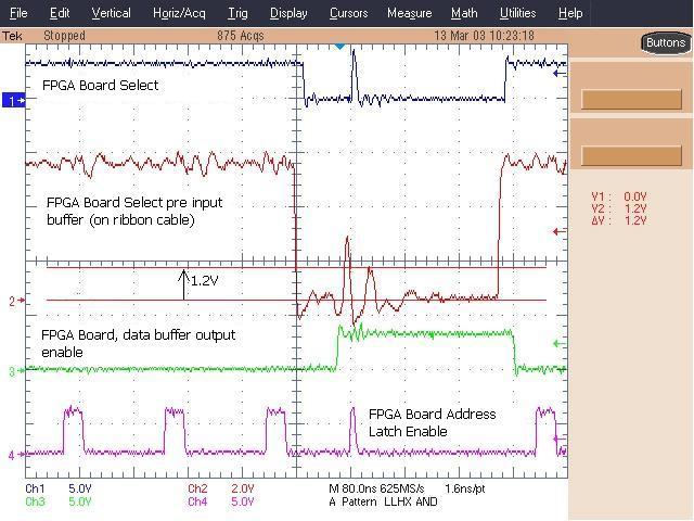
An example of the noise induced on the control lines when reading a word of 16 '1's is shown here.
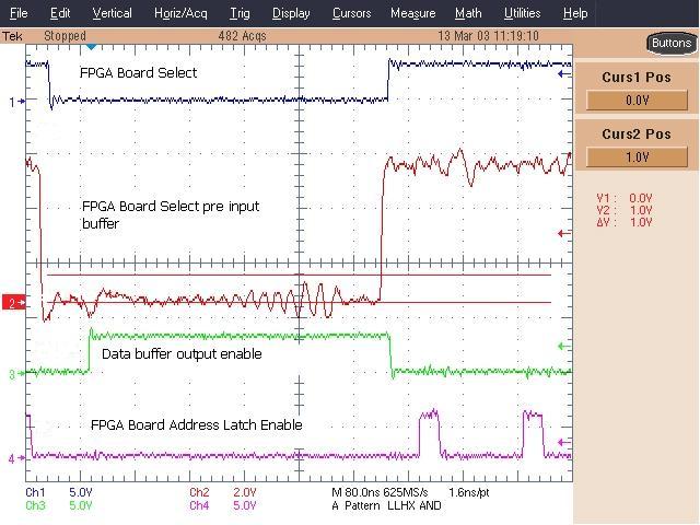
Luckily the uP used a configureable ChipSelect line to address the
FPGA board memory segment. It was possible to introduce wait states
to these accesses, and on any read from the FPGA the data bits were masked out from the
FPGA one at a time.
With this configuration the noise induced on the
interface lines was still present, but never sufficiently bad to cause spikes on any control
lines. The results of this modification are shown below (the influence of the bits nearest
the control lines is clearly seen to be stronger than those furthest away). This again was a
'worst case' read of 16 '1's from a data register.
After thorough testing of the uP <-> FPGA board interface attention
then turned to the rest of the FPGA design. As stated above the P+R tools
were reporting a maximum speed of 28MHz and the FPGA was being clocked at
50MHz. Our recommendation was to re-write the whole design as it was thought
faster than trying to debug the original (largely undocumented) design. The re-written design
was completely synchronous, all asynchronous external signals
were immediately re-timed to the 50MHz clock and the P+R tools reported
a maximum speed of 60MHz. Testbenches were written for functional verification of all modules
during the re-design, and when completed a complete design description was produced.
After some system tweaking and software optimisation the performance of
the system exceeded initial expectations. Aspects customers now have a
solid reliable system and are reported to be very happy with the results.
"Thanks again for all the good work you did in getting the SmartStation FPGA
code into good shape. It was a pleasure working with you and if we need any
more FPGA work, I know where to come."
Project Manager, Aspects Software.
Guidance Control Systems
Device Re-targeting
We were contacted by Guidance Control Systems who had a couple of legacy
designs targeted at Xilinx coolrunner parts written in ABEL. Xilinx had
discontinued the parts, Atmel provided a pin compatible part, but the
Atmel tools didn't support ABEL.
The designs were re-written by us in VHDL and re-targeted at the Atmel
devices. Despite this taking considerably longer than initially thought
(including fighting the vagaries of the Atmel tools) this work was
completed to the original quoted price.
"Nial Stewart Developments have been able to help us very quickly over come
problems of obsolescent programmable devices by translating our equation
files to VHDL and providing us with JED files ready for programming."
John Potter, GCS Ltd.
Coherent Micro Solutions
Custom FPGA Design/Development
Coherent Micro were develping a PCI card based product for the Oil and Gas
industry to reliably monitor pulses from turbines measuring oil flow and
direction. This was based on an Intel i960 uP with a Xilinx SpartanII to
measure pulse widths and inter-pulse timing from 8 turbine input channels.
When a pulse was received the relevant timings were calculated and the
uP interrupted. To ensure interrupts weren't missed an interrupt 'stack'
of up to seven events was implemented for each source. Outputs from the
design were triggered by writes to the relevant output registers.
We worked with Coherent Micro to produce a specification for the design from
a rough outline or required functionality. The design was written and documented
with testbences for verification. Our deliveries to Coherent Micro were a complete
project archive of all source files, testbenches, a design description and compile
scripts to allow the project to be easily modified and re-compiled.
"NSD worked with us to define our FPGA design requirements then quickly
provided a working design package and support.
Outsourcing this FPGA development to NSD allowed us to concentrate our
resources on other aspects of our system design allowing us to complete
our development more quickly."
David McKelvie, Coherent Micro Ltd


